- 您现在的位置:买卖IC网 > Sheet目录1223 > KIT10XS3535EVBE (Freescale Semiconductor)KIT EVAL BOARD FOR 10XS3535
�� �
�
�FUNCTIONAL� DEVICE� OPERATION�
�OPERATIONAL� MODES�
�FUNCTIONAL� DEVICE� OPERATION�
�OPERATIONAL� MODES�
�SLEEP� MODE�
�The� Sleep� mode� is� the� default� mode� of� the� 10XS3535.�
�This� is� the� state� of� the� device� after� first� applying� battery�
�voltage� (V� BAT� )� and� prior� to� any� I/O� transitions.� This� is� also� the�
�state� of� the� device� when� IGN,� FOG,� FLASHER,� and� RST� are�
�logic� [0]� (wake=0).� In� the� Sleep� mode,� the� outputs� and� all�
�internal� circuitry� are� OFF� to� minimize� current� draw.� In�
�addition,� all� SPI-configurable� features� of� the� device� are� reset.�
�The� 10XS3535� will� transit� to� two� modes� (Normal� and� Fail)�
�depending� on� wake� and� fail� signals� (see� Fig13).�
�The� transition� to� the� other� modes� is� according� following�
�signals:�
�?� Wake� =� IGN� or� IGN_ON� or� FLASHER� or�
�FLASHER_ON� or� RST� or� FOG� or� FOG_ON�
�?� Fail� =� VCC� fail� or� SPI� fail� or� External� limp�
�NORMAL� MODE�
�The� 10XS3535� is� in� Normal� mode� when:�
�?� Wake� =� 1�
�?� Fail� =� 0�
�I� n� Normal� operating� mode� the� power� outputs� are� under� full�
�control� of� the� SPI� as� follows:�
�?� The� outputs� 1� to� 6,� including� multiphase� timing� and�
�selectable� slew-rate,� are� controlled� by� the�
�programmable� PWM� module.�
�?� The� outputs� 1� to� 5� are� switched� OFF� in� case� of� an�
�under-voltage� on� VBAT.�
�?� The� outputs� 1� to� 5� are� protected� by� the� selectable� over-�
�current� double� window� and� over-temperature� shutdown�
�circuit.�
�?� The� digital� diagnosis� feature� transfers� status� of� the�
�smart� outputs� via� SPI.�
�D7� bit�
�D0-D6� bits�
�Output�
�Over-current�
�FAIL� MODE�
�The� 10XS3535� is� in� Fail� mode� when:�
�?� Wake� =� 1�
�?� Fail� =� 1�
�I� n� Fail� mode:�
�?� The� outputs� are� under� control� of� external� pins� (see�
��?� The� outputs� are� fully� protected� in� case� of� an� overload,�
�over-temperature� and� under-voltage� (on� VBAT� or� on�
�VCC).�
�?� The� SPI� reports� continuously� the� content� of� address� 11,�
�disregard� to� previous� requested� output� data� word.�
�?� Analog� current� sense� is� not� available.�
�?� Output� 2� is� configured� in� Xenon� mode.�
�?� In� case� of� an� overload� (OCHI2� or� OCLO)� conditions� or�
�under-voltage� on� VBAT,� the� outputs� are� under� control�
�of� autorestart� feature.�
�?� In� case� of� serious� overload� condition� (OCHI1� or� OT)� the�
�corresponding� output� is� latched� OFF� until� a� new� wake-�
�up� event� (wake=0� then� 1).�
�IGN_ON�
�?� The� analog� current� sense� output� (current� recopy�
�feature)� can� be� routed� by� SPI.�
�?� The� outputs� 1� and� 5� can� be� configured� to� control� LED�
�loads:� R� DS(ON)� is� increased� by� a� factor� of� 2� and� the�
�current� recopy� ratio� is� scaled� by� a� factor� of� 4.�
�?� The� SPI� reports� NM=1� in� this� mode.�
�IGN� (external)�
�OUT[1,2]�
�Over-current�
�1.4� sec� min�
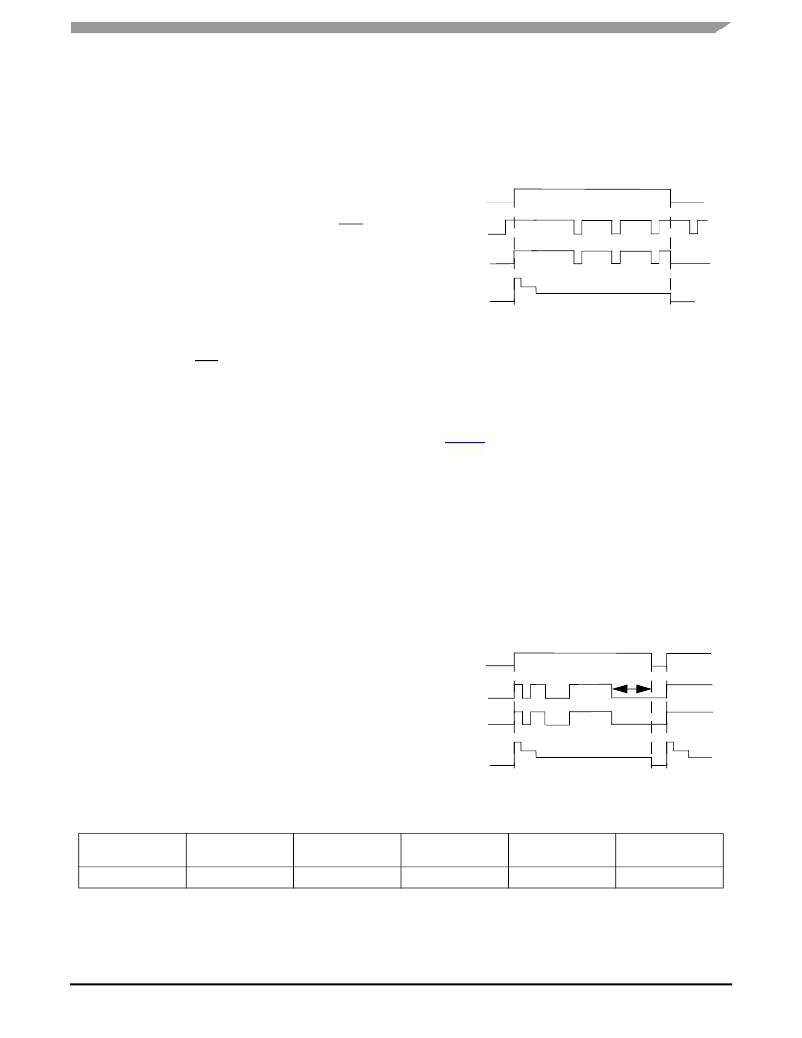
�The� figure� below� describes� the� PWM,� outputs� and� over-�
�current� behavior� in� Normal� mode.�
�Table� 6.� Limp� Home� Output� State�
�Output� 1�
�Parking� Light�
�IGN� Pin�
�Output� 2�
�Low� Beam�
�IGN� Pin�
�Output� 3�
�High� Beam�
�OFF�
�Output� 4�
�Fog� Light�
�FOG� Pin�
�Output� 5�
�Flasher�
�FLASHER� Pin�
�External� Switch�
�Spare�
�OFF�
�MC10XS3535�
�Analog� Integrated� Circuit� Device� Data� ?�
�Freescale� Semiconductor�
�25�
�发布紧急采购,3分钟左右您将得到回复。
相关PDF资料
KIT13892VLEVBEJ
KIT EVAL FOR MC13892
KIT17C724EPEVBE
KIT FOR 17C7242CH HBRIDGE PWR IC
KIT33810EKEVME
BOARD EVAL FOR MC33810
KIT33811EGEVBE
KIT EVAL 33811 SOLENOID MON IC
KIT33812ECUEVME
KIT DESIGN FOR 33812/S12P
KIT33812EKEVBE
BOARD EVALUATION FOR MC33812
KIT33879AEKEVBE
BOARD EVALUATION FOR MC33879
KIT33880DWBEVB
KIT EVAL FOR MC33880 8X SW W/SPI
相关代理商/技术参数
KIT10XS4200EVBE
制造商:Freescale Semiconductor 功能描述:EVAL BOARD, MC10XS4200 HIGH SIDE SWITCH; Silicon Manufacturer:Freescale; Silicon Core Number:MC10XS4200; Kit Application Type:High Side Switch; Application Sub Type:-; Kit Contents:Eval Board MC10XS4200, CD ROM
KIT-1113C
制造商:ABIKO 功能描述:Bulk
KIT1116-400
制造商:Laird Technologies Inc 功能描述:ANTKIT,FG 128-137MHZ/ODB + FM2
KIT-113-175C
制造商:LG Corporation 功能描述:KIT TUNER 113-175C (113-175E +
KIT1133-P250
功能描述:ANTKIT GB8W15FT CABLE 制造商:laird technologies ias 系列:* 零件状态:在售 标准包装:1
KIT-11591
功能描述:ISP POGO ADAPTER KIT 制造商:sparkfun electronics 系列:- 零件状态:在售 套件类型:初级入门套件 主要用途:ISP Pogo 适配器 标准包装:1
KIT1167-120
制造商:Laird Technologies Inc 功能描述:ANT KIT GPS1575PW 20FT 制造商:Laird Technologies Inc 功能描述:ANTKIT,GPS1575PW/20FT
KIT1185-120
制造商:Laird Technologies Inc 功能描述:KIT ANT GPS 20FT 制造商:Laird Technologies Inc 功能描述:KIT1185-120